🍟 The State of Open-Source EDA Tools for ASIC Design
Democratising silicon: from RTL to GDSII without a million-dollar licence

The Design Cost Crisis
For decades, the semiconductor industry operated under an implicit assumption: if you wanted to design custom silicon, you needed access to commercial Electronic Design Automation (EDA) tools costing hundreds of thousands to millions of dollars annually. This financial barrier created an ecosystem where only large corporations and well-funded research institutions could participate in chip design, effectively locking out startups, hobbyists, and researchers in developing nations.
Professor Andrew Kahng of UC San Diego frames this challenge starkly.1 In his keynote at the EFCL Summer School 2024, he presented Andreas Olofsson's analysis showing the exponentially rising cost of designing silicon at leading nodes. The trajectory is alarming: design costs have scaled from tens of millions at mature nodes to hundreds of millions at advanced processes, with predictions suggesting billion-dollar design costs at the most aggressive nodes. This represents what Kahng terms "the crisis of design" -- innovation in silicon runs into barriers of cost, expertise, and risk that prevent system architects and chip designers from exploring hardware realisation.
Design-Based Scaling
The semiconductor industry has relied on "design-based equivalent scaling" to maintain the value proposition of new technology nodes. As intrinsic scaling benefits diminish, EDA and design methodology carry the primary burden of extracting value from each new generation.
The economics are particularly punishing for academic research. When every PhD student must sign non-disclosure agreements with tool vendors, when license costs exceed departmental budgets, when results cannot be independently reproduced or benchmarked, the scientific method itself becomes compromised. As Kahng observes, the tragedy has been watching students attempt to reconstruct thousands of lines of code from fifteen lines of pseudocode in a conference paper, reinventing fundamental building blocks like buffer insertion or placement legalisation because no shared infrastructure exists.
The Open-Source Revolution
The landscape began shifting in 2018 when DARPA funded the OpenROAD project, recognising that open-source EDA could address the design cost crisis whilst maintaining American leadership in semiconductor technology. The program's deliverable was ambitious: an automated RTL-to-GDSII tool capable of push-button, tapeout-clean layout in commercial FinFET nodes, released under a permissive open-source licence.
What emerged was not merely a collection of academic prototypes, but production-quality tools now used in over 600 silicon-ready tapeouts across technologies up to 12nm.2 The OpenROAD flow integrates synthesis (via Yosys), floorplanning (TritonFPlan), placement (Replace/DGReplace), clock tree synthesis, detailed routing (TritonRoute), parasitic extraction (OpenRCX), and static timing analysis (OpenSTA) into a cohesive autonomous flow.
A Paradigm Shift
Open-source EDA is not merely cheaper commercial EDA. It enables fundamentally different approaches: unlimited tool runs for design space exploration, transparent heuristics that can be understood and improved, freedom to benchmark and compare, and data sharing for machine learning research.
The philosophical shift matters as much as the technical one. Kahng emphasises that "open really means open" -- there is no such thing as "open but not for use by people who hold certain passports." This characteristic makes open-source EDA particularly valuable in an era of export controls and geopolitical semiconductor competition, enabling genuine global collaboration whilst paradoxically supporting regional sovereignty goals.
The Tool Ecosystem
Understanding the open-source EDA landscape requires appreciating both the individual tools and their integration into complete flows. Unlike commercial EDA, where a single vendor typically provides a monolithic solution, open-source EDA assembles best-of-breed components into customisable toolchains.
Further Reading on ASIC Design Flows
For a comprehensive overview of open-source EDA tools and the ASIC design process, see AnySilicon's Ultimate Guide to Open Source EDA Tools. For those coming from an FPGA background, the companion post on Open-Source FPGA Tools provides useful context on synthesis and verification tools that share heritage with ASIC flows.
The following diagram illustrates the end-to-end ASIC design flow, from RTL specification through to manufacturable GDSII, with the primary open-source tools handling each stage:
%%{init: {'flowchart': {'padding': 20, 'nodeSpacing': 30, 'rankSpacing': 40}}}%%
flowchart TD
    RTL["RTL / Verilog"] --> YOSYS
    CONST["Constraints"] --> YOSYS
    PDK["PDK"] --> YOSYS
    PDK --> FLOOR

    YOSYS["Yosys<br/>Synthesis"] -->|Netlist| FLOOR

    FLOOR["Floorplanning"] --> PLACE["Placement"]
    PLACE --> CTS["Clock Tree<br/>Synthesis"]
    CTS --> ROUTE["Routing"]

    ROUTE --> STA["STA"] & DRC["DRC"] & LVS["LVS"]

    STA & DRC & LVS --> GDSII["GDSII"]

    GDSII --> FAB["Fabrication"]

    style RTL fill:#e1f5fe,stroke:#0288d1,color:#01579b
    style CONST fill:#e1f5fe,stroke:#0288d1,color:#01579b
    style PDK fill:#e1f5fe,stroke:#0288d1,color:#01579b
    style YOSYS fill:#fff3e0,stroke:#f57c00,color:#e65100
    style FLOOR fill:#e8f5e9,stroke:#388e3c,color:#1b5e20
    style PLACE fill:#e8f5e9,stroke:#388e3c,color:#1b5e20
    style CTS fill:#e8f5e9,stroke:#388e3c,color:#1b5e20
    style ROUTE fill:#e8f5e9,stroke:#388e3c,color:#1b5e20
    style STA fill:#fce4ec,stroke:#c2185b,color:#880e4f
    style DRC fill:#fce4ec,stroke:#c2185b,color:#880e4f
    style LVS fill:#fce4ec,stroke:#c2185b,color:#880e4f
    style GDSII fill:#f3e5f5,stroke:#7b1fa2,color:#4a148c
    style FAB fill:#f3e5f5,stroke:#7b1fa2,color:#4a148c
Colour key: Design Inputs | Synthesis | Physical Design (OpenROAD) | Sign-off | Output
Synthesis: Yosys

Yosys (Yosys Open SYnthesis Suite) forms the synthesis foundation for most open-source ASIC flows.3 Originally developed by Clifford Wolf (now Claire Xenia Wolf) and maintained by YosysHQ, it implements a framework for Verilog RTL synthesis with extensive Verilog-2005 support and growing SystemVerilog capabilities through the UHDM plugin developed by Antmicro.
Yosys operates through a series of passes that transform and optimise the design representation. The tool reads Verilog, elaborates the design hierarchy, performs technology-independent optimisations, and maps to target-specific cell libraries. For ASIC flows, it accepts Liberty format (.lib) files describing standard cell timing and functionality, producing gate-level netlists suitable for physical implementation.
The framework's flexibility extends beyond pure synthesis. Yosys supports formal equivalence checking through SAT solving, enabling verification that RTL and gate-level representations remain functionally equivalent. This capability proves essential for design flows where synthesis transformations must be validated against specification.
Physical Design: OpenROAD

OpenROAD provides the physical implementation backbone, handling everything from floorplanning through detailed routing. The project represents the largest coordinated open-source EDA effort, with over 22,000 commits from 110 contributors and active maintenance by Precision Innovations.
The flow begins with floorplanning, where the hierarchical RTL macro placer (RTLMP) understands design hierarchy and dataflow to produce human-expert-like results. This tool has demonstrated superior results to commercial alternatives for certain design classes, particularly those with complex macro arrangements. For an AI accelerator with 760 macros in GlobalFoundries 12nm, the open-source macro placer dominated an unnamed commercial tool's placement when evaluated through complete place-and-route with identical downstream tools.
Standard cell placement employs Replace (RePlAce: Advancing Solution Quality and Routability Validation in Global Placement), with GPU-accelerated variants like DGReplace achieving placement of 800,000 instances in 32 seconds. This performance enables auto-tuning approaches that were previously impractical, allowing exploration of hyperparameter spaces to optimise power, performance, and area (PPA) objectives.
Clock tree synthesis and detailed routing complete the physical implementation, with TritonRoute handling the complex task of generating manufacturing-compliant metal interconnect. The flow produces GDSII output suitable for fabrication, with integrated design rule checking to ensure manufacturing compatibility.
Circuit Simulation: Ngspice
For analog and mixed-signal design, Ngspice provides SPICE simulation capabilities as the open-source successor to Berkeley SPICE. The tool combines three foundational packages: Spice3f5 for core circuit simulation, XSPICE for mixed-mode simulation with digital circuit models, and Cider1b1 for device-level numerical simulation.
Ngspice supports the full range of SPICE analyses: DC operating point, AC frequency response, transient time-domain behaviour, and noise analysis. Integration with schematic capture tools like KiCAD enables a complete analog design flow from schematic entry through simulation verification.
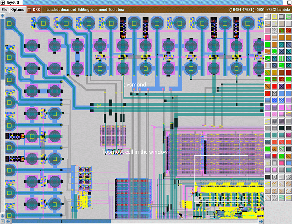
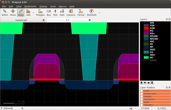
Layout Tools: Magic and KLayout
Physical layout and verification employ tools with deep heritage. Magic, developed at UC Berkeley in the 1980s, remains the most accessible tool for transistor-level layout with integrated design rule checking and layout versus schematic comparison. Its understanding of fabrication rules enables real-time DRC feedback during layout creation.
KLayout provides a modern layout editor supporting GDSII and OASIS formats with cross-section visualisation and extensive scripting capabilities through Python and Ruby APIs. The tool excels at viewing, editing, and analysing completed layouts, complementing Magic's strength in interactive layout creation.
Process Design Kits: SkyWater and GlobalFoundries
Tools alone cannot produce manufacturable designs; they require Process Design Kits (PDKs) describing the fabrication process. Google's partnership with SkyWater Technology revolutionised access by releasing SKY130, a fully open-source PDK for SkyWater's 130nm mixed-signal CMOS process.4 For those interested in the foundry's journey from Cypress Semiconductor spin-off to open-source champion, AnySilicon provides a detailed history of SkyWater Technology.
The SKY130 PDK provides everything needed for design: SPICE models for circuit simulation, design rules for layout verification, standard cell libraries, I/O cells, and memory compilers. Critically, designs created with SKY130 can be fabricated through programs like Tiny Tapeout and ChipIgnite, closing the loop from concept to physical silicon.
Educational Access
More than 50 universities now use the SKY130/Efabless platform for coursework, capstone projects, and research. Students can go from design concept to tapeout for as little as $50 through Tiny Tapeout, democratising hands-on semiconductor education.
GlobalFoundries subsequently released GF180MCU, providing an alternative open-source PDK at 180nm. Both PDKs have joined the Linux Foundation's CHIPS Alliance under a working group fostering continued open-source PDK development.
Complete Design Flows
Individual tools integrate into complete flows through wrapper frameworks that manage data flow and configuration. Several options exist, each with distinct philosophies and target applications.
OpenLane / LibreLane
Developed by Efabless, OpenLane provides an automated RTL-to-GDSII flow built on OpenROAD, Yosys, Magic, Netgen, and custom methodology scripts. The flow emphasises no-human-in-the-loop operation, automatically balancing PPA trade-offs to generate hardware without requiring extensive design experience.
OpenLane to LibreLane
The open-source community has forked OpenLane as LibreLane to ensure continued community-driven development. LibreLane maintains compatibility with existing OpenLane configurations whilst providing an independent development path.
OpenLane operates through a series of stages: synthesis with Yosys, floorplanning and placement with OpenROAD, clock tree synthesis, routing, GDSII generation with Magic, and verification with Netgen for LVS and Magic for DRC. Configuration through TCL files allows customisation whilst maintaining sensible defaults for common design patterns.
ORFS (OpenROAD-flow-scripts)
For users seeking more control, OpenROAD-flow-scripts provides a makefile-based flow enabling rapid architecture and design space exploration. ORFS emphasises flexibility for research applications, supporting multiple PDKs and allowing fine-grained control over each flow stage.
Qflow
The original open-source digital flow, Qflow predates OpenROAD and provides a simpler integration of Yosys, Graywolf (placement), QRouter (routing), and Magic. Though superseded by OpenROAD for advanced applications, Qflow remains valuable for educational contexts and simple designs.
Alliance/Coriolis
The Alliance VLSI CAD Tools, developed in France, provide an alternative end-to-end toolchain converting HDL input to GDSII output. Coriolis serves as the modern successor, implementing hierarchical design flows with particular strength in regular structures.
The Optimisation Imperative
At its core, IC design is optimisation: achieving the best possible results given limited resources of compute time, engineering effort, and silicon area. Kahng emphasises this fundamental truth repeatedly -- EDA exists to solve intractable optimisations at huge scale. Commercial tools have accumulated decades of heuristics, creating what he terms "chaos": negligible perturbations to input conditions can cause dramatic changes in output quality that no one on the planet can explain.
Experimental evidence quantifies this chaos. For an AES encryption core in GlobalFoundries 12nm, stepping the target clock period in synthesis by 0.01 picoseconds -- one-hundredth of a picosecond -- across a 2-picosecond interval produces 3.4% variation in effective clock period, 38% variation in leakage power, and 11% variation in total area. These variations represent an entire technology node of difference from tool noise alone.
The only mitigation is sampling: running many tool invocations hoping to find solutions in the good tail of the quality distribution. Open-source EDA enables this sampling where commercial licensing makes it prohibitively expensive. When a license costs six figures annually, running thousands of synthesis experiments becomes untenable. When the tool is free, the bottleneck shifts to compute resources that cloud infrastructure can readily provide.
ML-Enabled Optimisation
Auto-tuning approaches from machine learning, like those used in Cadence Cerebrus or Synopsys DSO.ai, become accessible when open-source tools enable unlimited experimentation. OpenROAD has included its own auto-tuner for several years, enabling hyperparameter optimisation without licensing constraints.
Machine Learning and the Data Problem
The intersection of machine learning and EDA represents perhaps the most significant opportunity enabled by open-source tools. Commercial EDA creates insurmountable barriers to ML research: proprietary PDK data cannot be shared, tool report formats are copyrighted, modelling tool behaviour may constitute reverse engineering, and license agreements contain export control clauses preventing collaboration.
Kahng frames this starkly: if you need a FlexLM license, if every student must sign NDAs with tool vendors, if documentation and outputs are proprietary, it means no benchmarking, no uploading into ChatGPT for analysis, no commercialisation of student chip designs. These barriers do not exist with open-source tools.
The importance of open infrastructure became apparent following Google DeepMind's AlphaChip work, which demonstrated reinforcement learning for chip placement. While the results were impressive, the proprietary nature of the system sparked significant debate about reproducibility. Critics questioned whether claims could be verified without access to the underlying infrastructure, prompting the original authors to publish "That Chip Has Sailed" defending their methodology. Regardless of where one stands on this debate, it underscores a fundamental truth: ML-EDA research requires open, reproducible infrastructure.

The ML-EDA research community has historically lacked the infrastructure that accelerated progress in other domains -- no ImageNet for chip design, no Hugging Face for EDA models, no shared pretrained representations. This is now changing. CircuitNet provides an open dataset of netlists, timing data, and layout information specifically designed for ML research, addressing the data scarcity that has hampered progress. A 2023 NSF workshop on shared infrastructure for ML-EDA proposed the SLICE framework to parallel the AI ecosystem's open infrastructure with pre-trained models, shared datasets, and community benchmarks.
On the tooling side, open-source ML-enabled EDA tools are maturing rapidly. DREAMPlace, developed at UT Austin, provides GPU-accelerated placement using deep learning techniques, achieving orders-of-magnitude speedups over traditional placers. NVIDIA's open-source CircuitOps platform leverages OpenROAD to model chip data as labelled property graphs and pandas DataFrames, streamlining integration of ML algorithms.
OpenROAD itself provides key infrastructure enabling ML-EDA research. Python APIs wrap underlying C++ engines, enabling faster data generation compared to commercial tools' TCL interfaces. These APIs also enable ML inference results to be integrated back into the database, closing the feedback loop essential for learning-based optimisation.
Educational Impact
Perhaps the most immediate impact of open-source EDA comes in education. Matt Venn's Tiny Tapeout program has demonstrated that 30 people can go from zero to tapeout on SkyWater 130nm using open-source tools in three hours. Of the hundreds who have taken Tiny Tapeout-based trainings, over 60% are students, teachers, researchers, or from industry. This frictionless onboarding represents a fundamental shift in semiconductor education.
The contrast with commercial tool access is stark. Students using open-source tools simply download and run, freely sharing projects without paperwork. UC Santa Cruz extension courses now teach open-source EDA alongside commercial tools. Training programs span from high school through universities in New York State. VLSISystemDesign in India and Zero to ASIC in Europe provide structured curricula built entirely on open-source foundations.
This educational democratisation addresses a critical workforce challenge. As semiconductor manufacturing investment accelerates globally through programs like the US CHIPS Act and European Chips Act, the industry faces severe talent shortages. Open-source EDA tools provide the on-ramp for training the next generation without requiring institutions to negotiate enterprise license agreements.
Technical Comparison: Open vs Commercial
Honest assessment requires acknowledging the current quality gap. Commercial EDA tools, refined over decades with billions of investment, produce better quality of results in most scenarios. Kahng presents this graphically: the blue Pareto frontier of open-source tools sits above and to the right of the red commercial frontier on plots of timing versus area.
However, this gap tells only part of the story. First, nobody knows where optimal lies -- both curves may be far from theoretical limits. Second, open-source tools improve rapidly when unlimited experimentation enables ML-guided optimisation. Third, hybrid flows combining open and commercial tools often outperform either alone, using free tools for exploration and commercial tools for final implementation.
| Aspect | Commercial EDA | Open-Source EDA |
|---|---|---|
| PPA Quality | Superior at leading nodes | Competitive at mature nodes |
| Cost | \(100K-\)1M+ annually | Free (compute costs only) |
| Node Support | All commercial nodes | SKY130, GF180, ASAP7, GF12 |
| Documentation | Comprehensive but proprietary | Variable, improving |
| Support | Commercial support available | Community and commercial options |
| Flexibility | Limited customisation | Full source access |
| Benchmarking | Prohibited by license | Unrestricted |
| ML Research | Severely constrained | Fully enabled |
For certain applications, open-source tools already match or exceed commercial alternatives. The hierarchical RTL macro placer in OpenROAD demonstrated superior results on complex macro-heavy designs. GPU-accelerated placement enables exploration impossible with commercial license constraints. Design space exploration and early PPA estimation benefit more from speed than absolute quality.
The Path Forward
Open-source EDA exists in a virtuous cycle: better tools attract more users, more users generate more data, more data enables better ML models, better models improve tools. This flywheel parallels the dynamics that drove rapid progress in natural language processing and computer vision, spinning faster on the exhaust of openly shared data.
Several technical frontiers demand attention. Analog and mixed-signal design remains less mature than digital flows, limiting system-on-chip integration. RF design tools are nascent. Multi-die integration and chiplet assembly planning lack comprehensive solutions. Sign-off quality analysis still relies heavily on commercial tools for production designs.
The organisational model continues evolving. Precision Innovations provides commercial support for OpenROAD, demonstrating that open-source EDA can sustain viable businesses. The CHIPS Alliance working group coordinates PDK development. University research groups contribute algorithmic innovations. The ecosystem requires coordination, patience, and sustained investment -- as Kahng notes, there is simply too much to be done for fragmented efforts.
Historical Context
The Design Automation Conference originated as the "SHARE Design Automation Workshop" -- SHARE standing for "Society to Help Avoid Redundant Efforts." This founding philosophy of collaboration over duplication captures what open-source EDA must achieve.
Practical Considerations
For those considering open-source EDA tools, several practical factors merit consideration.
Target Technology: Open-source PDKs currently support mature nodes (130nm-180nm) with academic research PDKs like ASAP7 providing 7nm-equivalent models for research. Production designs at leading nodes still require commercial PDKs and typically commercial tools.
Design Complexity: Simple digital designs are straightforward. Complex SoCs with mixed-signal integration, custom memory, or aggressive timing constraints may require hybrid flows or commercial tools for final implementation.
Compute Resources: The freedom to run unlimited experiments creates compute bottlenecks rather than license bottlenecks. Cloud infrastructure integration enables scaling experimentation.
Community Support: Active communities on GitHub, Discord, and mailing lists provide support. Precision Innovations offers commercial support contracts for production users.
Learning Curve: Documentation has improved substantially but remains less polished than commercial tool suites. The Coursera "Introduction to Chip Design with Open Source EDA Tools" course provides structured learning covering Magic, KiCAD, Ngspice, and OpenROAD.
Conclusion
The semiconductor industry stands at an inflection point. Commercial EDA tools remain essential for leading-edge production designs, but open-source alternatives now enable serious chip design for education, research, startups, and mature-node products. More fundamentally, open-source EDA changes the nature of design itself: enabling unlimited experimentation, transparent optimisation, reproducible research, and global collaboration.
The trajectory seems clear. As Matt Venn observed, you can now go from zero to tapeout in three hours with tools that cost nothing and constraints that prevent nothing. A student can design and fabricate a chip for $50. More than 600 designs have taped out using open-source flows. The tools downloaded over a thousand times daily represent a growing community of designers who need not ask permission to innovate.
For researchers, open-source EDA removes the barriers that prevented machine learning from transforming IC design. For educators, it provides friction-free access that commercial licenses could never match. For startups, it eliminates the capital requirement that gatekept entry. For established companies, it offers design space exploration impossible with license constraints.
The crisis of design cost that motivated DARPA's investment in OpenROAD has not been solved. Leading-edge chips still cost hundreds of millions to design. But the trajectory has changed. Open-source EDA demonstrates that alternatives exist, that quality improves rapidly with investment, and that democratised chip design is not merely possible but increasingly practical.
As Kahng reminded his audience in Zurich, the original Design Automation Conference was about helping avoid redundant efforts through sharing. Open-source EDA returns to those roots, building shared infrastructure that no single entity could justify alone. The question is no longer whether open-source EDA can produce manufacturable silicon -- hundreds of chips prove it can. The question is how quickly the ecosystem matures and how many innovators seize the opportunity it creates.
Further Resources
Courses and Tutorials
- Zero to ASIC Course - Matt Venn's comprehensive training program
- Tiny Tapeout - From design to silicon in hours for $50
- VLSISystemDesign - India-based training programs
- Coursera: Introduction to Chip Design - Structured learning with hands-on labs
Tools and Flows
- OpenROAD Project - RTL-to-GDSII autonomous flow
- OpenROAD-flow-scripts - Makefile-based design exploration flow
- Yosys - Open synthesis suite
- OpenLane - Efabless automated flow
- LibreLane - Community fork of OpenLane
- Magic VLSI - Layout tool
- Ngspice - SPICE simulation
- KLayout - Layout editor and viewer
ML-EDA Tools and Datasets
- CircuitNet - Open dataset for ML in chip design
- DREAMPlace - GPU-accelerated ML placement
- CircuitOps - NVIDIA's ML-EDA integration platform
Process Design Kits
- SkyWater SKY130 PDK - Open-source 130nm PDK
- GlobalFoundries GF180MCU - Open-source 180nm PDK
- ASAP7 PDK - Academic 7nm-equivalent research PDK
Community
- CHIPS Alliance - Linux Foundation working group
- FOSSi Foundation - Free and Open Source Silicon Foundation
- OpenROAD Birds of a Feather - DAC community gatherings
References
-
Kahng, A.B. (2024). "Accelerating Design Innovation." EFCL Summer School Keynote, ETH Zurich. ↩
-
Ajayi, T., et al. (2019). "OpenROAD: Toward a Self-Driving, Open-Source Digital Layout Implementation Tool Chain." GOMAC Tech. ↩
-
Wolf, C. (2016). "Yosys Open Synthesis Suite." Open Source Digital Design Conference. ↩
-
SkyWater Technology Foundry. (2020). "SkyWater Open Source PDK." GitHub Repository. ↩